M. Bag's Group at IIT Roorkee...
We are mainly working on inorganic-organic hybrid perovskite materials; towards improving the efficiencies of perovskite LEDs and perovskite solar cells.
Zahner impedance spectroscopy setup is used to study the energetics at various interfaces, understanding the band structure of materials.
Our purpose is to achive balanced charge injection and reduced leackage current at the interface. Our group is working towards the optimization of morphology of thin films
prepared by solution processed coating technique.
Any noise could be unwanted for common people but is important for us to understand optoelectronics devices. Like any other spectroscopic technique, Noise spectroscopy can unfold significant insight about charge transport properties in the devices. Along with Electrochemical Impedance Spectroscopy (EIS) and Intensity Modulated Photocurrent/Photovoltage Spectroscopy (IMPS/IMVS), our group focus on the Noise spectroscopy as alternative tool to understand charge carrier dynamics in various optoelectronics devices.
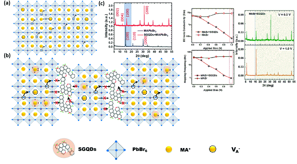
In this work, we have demonstrated that the ionic conductivity in perovskite/electrolyte based device depends on the interpaly between A-site cations and X-site halide ions. JPL behavior is observed at low-frequency to mid-frequency regime in the PEIS measurement while high frequency ac conductivity is frequency-indenpendent.
In this work, we have demonstrated that the composition of perovskite materials plays a significant role in controlling the electrical and ionic properties in mixed cation mixed halide (MCMH) perovskite-based devices. The most exciting finding is that the low frequency ionic conductivity follows opposite behavior for two MCMH devices due to the interplay between A-site cation and X-site halide ion.
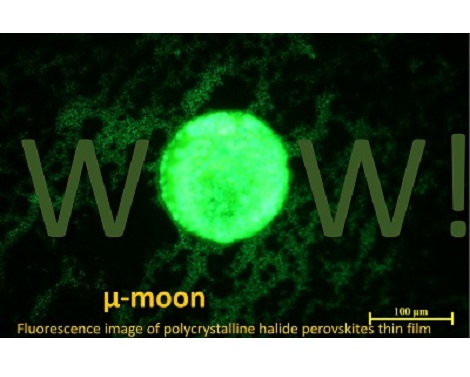
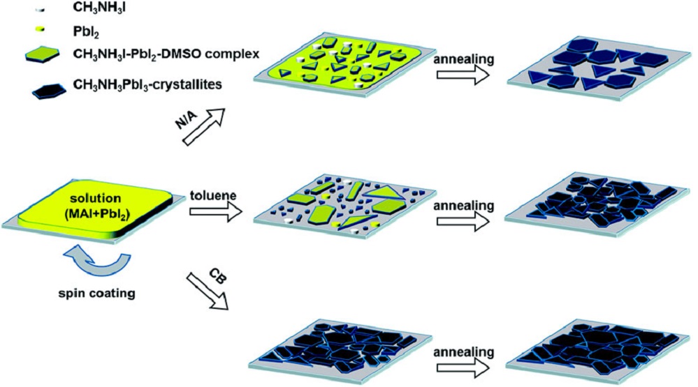
Our latest work explains the features of perovskite film morphology based on Stranski Krastanov Growth. In this publication, we have provided a clear picture of the growth mechanism of textured patterns, and by using a series of fluorescence measurements, we found that the nanostructured micro-islands exhibited superior emission and large quasi-Fermi level splitting.
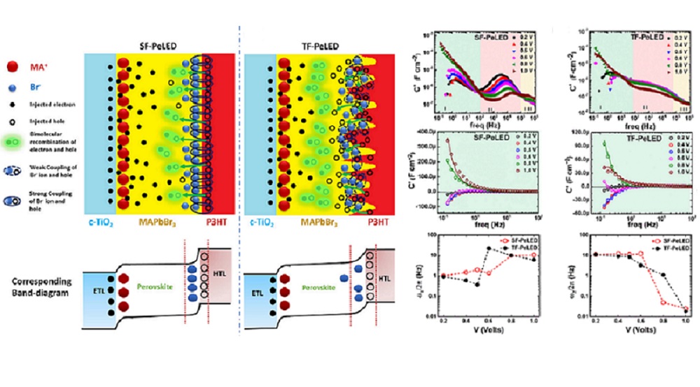
We have demonstrated the Negative capacitance in PeLEDs for the first time, that depends on morphology. Hope it will show a new way to rethink device physics.
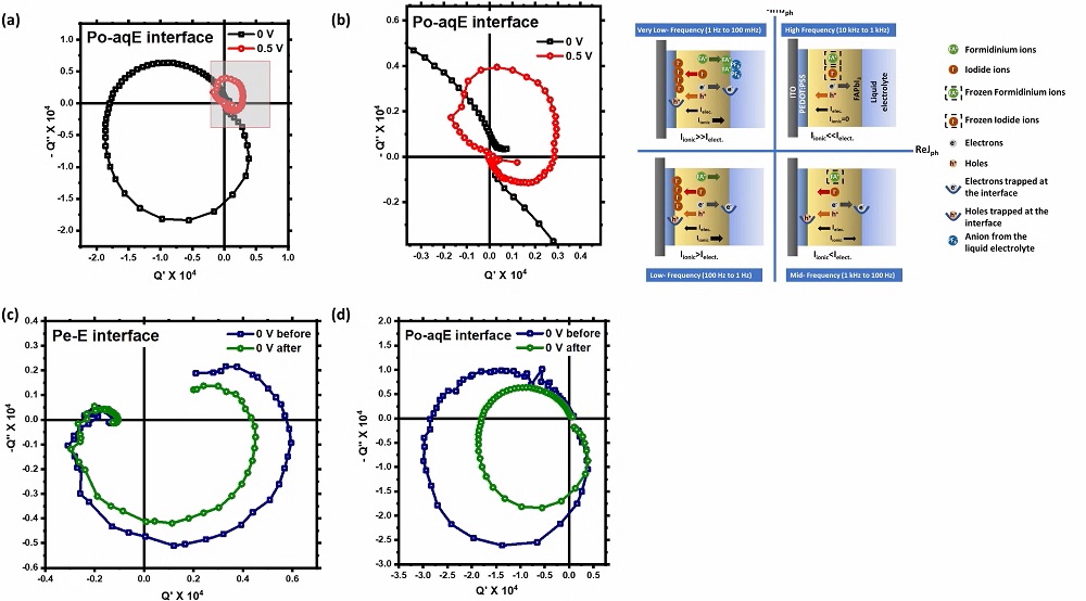
In this article we have investigated charge transport through a perovskite/electrolyte interface using electrochemical impedance spectroscopy (EIS) under illumination and applied bias conditions. Our results indicate ambipolar charge transport through the perovskite layer and field induced bleaching at the CH3NH3PbI3/electrolyte interface.
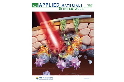
In this article we have investigated origin of voltage loss and charge trapping in surfactant stabilized nanoparticle based devices. This article is published in ACS Applied Materials and Interfaces.
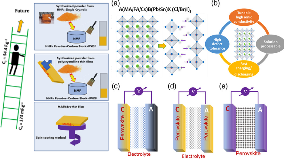
Happy to share our first book chapter Chapter No.5 : Ion Transport and Stability Issues in Organic–Inorganic Perovskite Materials in the book Revolution of Perovskites: Synthesis, Properties and Application by Springer Publication.